MT3620 reference development board (RDB) user guide
This topic describes user features of the MT3620 reference development board (RDB) v1.7.
- Programmable buttons and LEDs
- Four banks of interface headers for input and output
- Configurable power supply and two voltage regulators.
- Configurable Wi-Fi antennas
- Ground test point
The RDB design has undergone a number of revisions, and all the versions can be found in the Azure Sphere Hardware Designs Git repository. This document describes the latest version of the RDB (v1.7). For information on the previous RDB designs, see the MT3620 RDB user guide—v1.6 and earlier. If you have a development board that follows the RDB design and you want to know which version it is, see the MT3620 reference board design.
Buttons and LEDs
The board supports two user buttons, a reset button, four RGB user LEDs, an application status LED, a Wi-Fi status LED, a USB activity LED, a board power-on LED, and an MT3620 power-on LED.
The following sections provide details about how each of these buttons and LEDs connects to the MT3620 chip.
User buttons
The two user buttons (A and B) are connected to the GPIO pins listed in the following table. Note that these GPIO inputs are pulled high via 4.7K resistors. Therefore, the default input state of these GPIOs is high; when a user presses a button, the GPIO input is low.
| Button | MT3620 GPIO | MT3620 Physical Pin |
|---|---|---|
| A | GPIO12 | 27 |
| B | GPIO13 | 28 |
Reset button
The development board includes a reset button. When pressed, this button resets the MT3620 chip. It does not reset any other parts of the board. If the MT3620 is in PowerDown mode, pressing the reset button will wake the chip as the Reset button is also connected to the MT3620 WAKEUP signal.
User LEDs
The development board includes four RGB user LEDs, labeled 1-4. The LEDs connect to MT3620 GPIOs as listed in the following table. The common anode of each RGB LED is tied high; therefore, driving the corresponding GPIO low illuminates the LED.
| LED | Color Channel | MT3620 GPIO | MT3620 Physical Pin |
|---|---|---|---|
| 1 | Red | GPIO8 | 21 |
| 1 | Green | GPIO9 | 22 |
| 1 | Blue | GPIO10 | 25 |
| 2 | Red | GPIO15 | 30 |
| 2 | Green | GPIO16 | 31 |
| 2 | Blue | GPIO17 | 32 |
| 3 | Red | GPIO18 | 33 |
| 3 | Green | GPIO19 | 34 |
| 3 | Blue | GPIO20 | 35 |
| 4 | Red | GPIO21 | 36 |
| 4 | Green | GPIO22 | 37 |
| 4 | Blue | GPIO23 | 38 |
Application status LED
The application status LED is intended to provide feedback to the user about the current state of the application that is running on the A7. This LED is not controlled by the Azure Sphere operating system (OS); the application is responsible for driving it.
| LED | Color Channel | MT3620 GPIO | MT3620 Physical Pin |
|---|---|---|---|
| Application status | Red | GPIO45 | 62 |
| Application status | Green | GPIO46 | 63 |
| Application status | Blue | GPIO47 | 64 |
Wi-Fi status LED
The Wi-Fi status LED is intended to provide feedback to the user about the current state of the Wi-Fi connection. This LED is not controlled by the Azure Sphere OS; the application is responsible for driving it.
| LED | Color Channel | MT3620 GPIO | MT3620 Physical Pin |
|---|---|---|---|
| Wi-Fi Status | Red | GPIO48 | 65 |
| Wi-Fi Status | Green | GPIO14 | 29 |
| Wi-Fi Status | Blue | GPIO11 | 26 |
USB activity LED
The green USB activity LED blinks whenever data is sent or received over the USB connection. The hardware is implemented so that data sent or received over any of the four Future Technology Devices International (FTDI) channels causes the LED to blink. The USB activity LED is driven by dedicated circuitry and therefore requires no additional software support.
Power-on LEDs
The board includes two power-on LEDs:
- A red power-on LED that illuminates when the board is powered from USB or by an external 5V supply.
- A red MT3620 power-on LED that illuminates when the MT3620 is powered.
The LEDs are labeled with the following icons:
| Board power | MT3620 power |
|---|---|
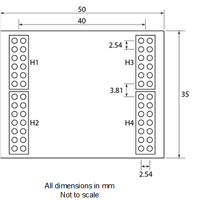
Interface headers
The development board includes four banks of interface headers, labeled H1-H4, which provide access to a variety of interface signals. The diagram shows the pin functions that are currently supported.
Note
For I2C, DATA and CLK in the diagram correspond to SDA and SCL. Pull-up I2C SCL and I2C SDA with 10K ohm resistors.

Daughter board
The headers are arranged to allow a daughter board (also referred to as a "shield" or "hat") to be attached to the RDB. The following diagram shows the dimensions of a typical daughter board, along with the locations of the headers.
Power supply
The MT3620 board can be powered from USB, an external 5V power source, or both. If both sources are simultaneously connected, circuitry prevents the external 5V supply from back-powering the USB.
The board includes protection against reverse voltage and overcurrent. If an overcurrent situation occurs, the protection circuit trips and isolates the incoming 5V supply from the rest of the board. Even if the fault that caused the overcurrent circuit to trip is removed, it will be necessary to disconnect the external power source (USB or ext. 5V) to the board to reset the overcurrent circuit.
The power source must be capable of supplying 600mA even though this much current is not requested during USB enumeration. The board draws around 225mA while running, rising to around 475mA during Wi-Fi data transfer. During boot and while associating to a wireless access point, the board may require up to 600mA for a short time (approximately 2ms). If additional loads are wired to the development board header pins, a source capable of supplying more than 600mA will be required.
The RDB includes two on-board 3.3V power supplies. The first powers just the MT3620 and the second powers the FTDI interface and other peripheral circuitry. The supply that powers the MT3620 can be configured to turn off when the MT3620 enters Power Down mode. The second power supply (such as for the FTDI) remains always on.
A CR2032 battery can be fitted to the board to power the internal real-time clock (RTC) of the MT3620 chip. Alternatively, an external battery can be connected to pin 2 of J3 as described under Jumpers.
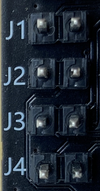
Jumpers
The board includes four jumpers (J1-J4) that provide a means of configuring power for the board. The jumpers are located towards the lower-left of the board; in each case, pin 1 is on the left:
Important
The MT3620 fails to operate correctly if the RTC is not powered.
The following table provides details about the jumpers.
| Jumper | Function | Description |
|---|---|---|
| J1 | ADC VREF | This jumper provides a way to set the ADC reference voltage. Place a link on J1 to connect the MT3620's 2.5V output to the ADC VREF pin, so that the ADC reference voltage is 2.5V. Alternatively, connect an external 1.8V reference voltage to pin 1 of the jumper. |
| J2 | MT3620 3V3 Isolation | This jumper provides a way to isolate the power that supplies the MT3620. For normal use, place a link on J2. To use an external 3.3V supply to power the MT3620, connect the external 3.3V supply to pin 2 of J2. J2 also provides a convenient connection point for external current measuring equipment, should the current consumption of the MT3620 need to be monitored. |
| J3 | RTC Supply | This jumper sets the power source for the MT3620's internal real time clock (RTC). With a link placed on J3, the RTC is powered from either the always-on 3.3V supply or the coin cell; depending on which of these two power sources is available, on-board circuitry automatically switches to the supply with the highest voltage. To power the RTC from an external source, remove the link and connect the source to pin 2 of J3. |
| J4 | MT3620 power supply control | With a link placed on J4, the MT3620's power supply will turn off when the MT3620 enters PowerDown mode. If you require the MT3620's power supply to remain on at all times, remove the link from J4. |
Power Down mode
The Azure Sphere operating system provides support for Power Down, which is a low-power state.
To achieve the lowest power consumption state when the MT3620 enters PowerDown mode, it is necessary for the MT3620's power supply to also be turned off. This is achieved by placing a link on jumper J4 which connects the EXT_PMU_EN signal (an output from the MT3620) to the enable pin of the power supply's voltage regulator. When the MT3620 enters PowerDown mode, the state of EXT_PMU_EN transitions from high to low, thus disabling the MT3620 voltage regulator.
The WAKEUP signal
WAKEUP is an MT3620 input that can be used to bring the chip out of Power Down mode. By default, the RDB pulls the WAKEUP signal high to the RTC supply, via a 4.7K resistor; pulling it low will bring the chip out of Power Down mode.
Wi-Fi antennas
The RDB includes two dual-band chip antennas and two RF connectors for connecting external antennas or RF test equipment. One antenna is considered the main antenna and the second is considered auxiliary. By default, the development board is configured to use the on-board main antenna; the auxiliary antenna is not currently used.
To enable and use the RF connectors, you must reorient capacitors C23, C89, or both. The first row in the following table shows the default configuration where the on-board chip antennas are in use, with the associated capacitor positions highlighted in red. The images on the second row show the re-oriented capacitor positions.
| Auxiliary antenna | Main antenna |
|---|---|
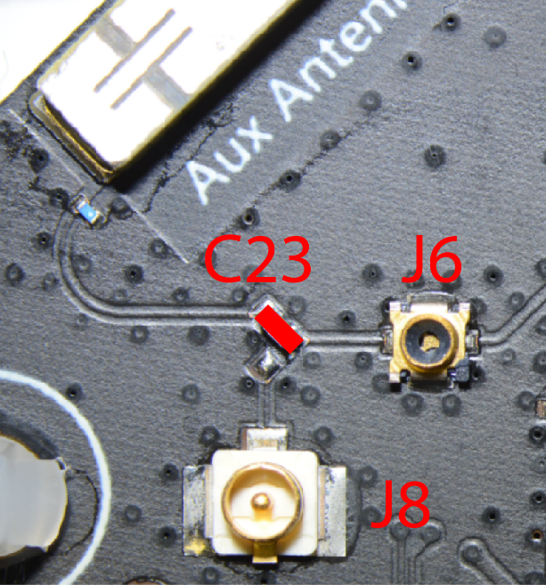 C23 default configuration, on-board chip antenna |
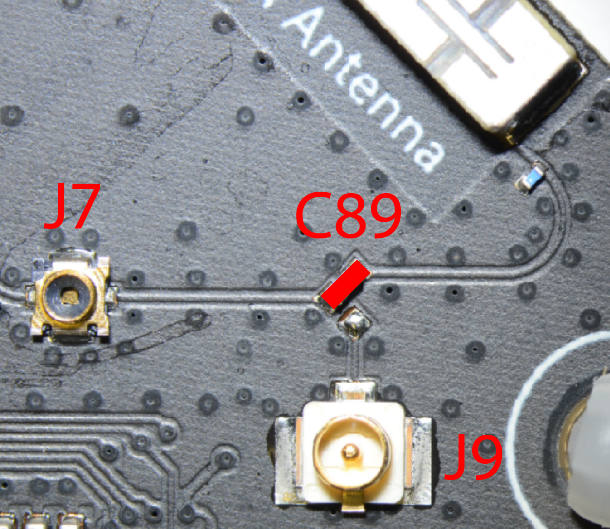 C89 default configuration, on-board chip antenna |
 C23 alternate configuration – external antenna connects to J8 |
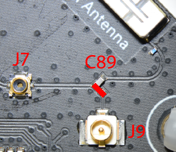 C89 alternate configuration – external antenna connects to J9 |
Note
Connectors J6 and J7 are used for RF testing and calibration during manufacture and are not intended for permanent connection to test equipment or external antennas.
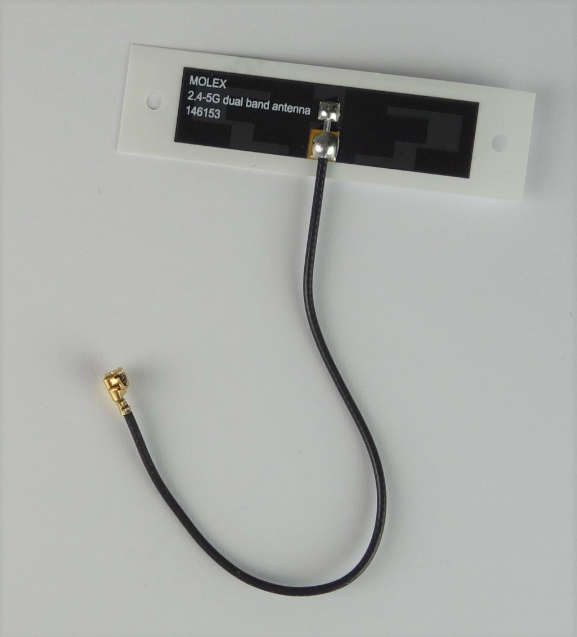
Any type of 2.4 or 5GHz external antenna with a U.FL or IPX connector can be used with the board, such as the Molex 1461530100 (pictured below). When fitting an external antenna, you are responsible for ensuring that all regulatory and certification requirements are met.
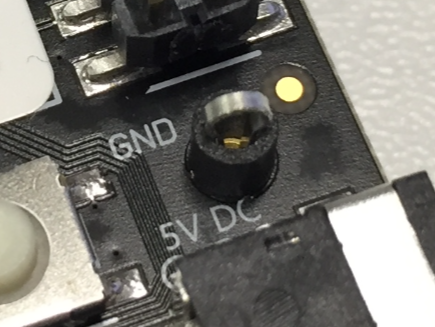
Ground test point
The MT3620 development board provides a ground test point on the right side, next to button B and immediately above the 3.5 mm barrel socket, as shown in the image. Use this during testing—for example, for attaching the ground lead of an oscilloscope probe.
Feedback
Coming soon: Throughout 2024 we will be phasing out GitHub Issues as the feedback mechanism for content and replacing it with a new feedback system. For more information see: https://aka.ms/ContentUserFeedback.
Submit and view feedback for